Showing posts with label Audio. Show all posts

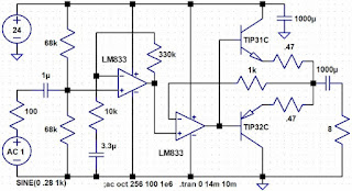
Simpler Hi-Fi Audio Amplifier Circuit Diagram

Here are Simpler Hi-Fi Audio Amplifier Circuit Diagram, If  you can settle for more distortion (from about 0.2% to 0.4% at full power) and about 2.5 watts into 8 ohms with a 20 to 24 VDC power supply, the following circuit is a lot simpler. The op-amp has to discharge the base of one transistor to turn it off while also trying to pump charge into the other transistor to turn it on, hence more distortion at crossover. The distortion isn't noticeable for many applications but it's significantly higher than the circuit above. I used a larger, 2200 uF capacitor across the power. If you experience instability try adding a few hundred pF capacitor to the second op-amp from the negative input to the output. This "local" feedback should keep the op-amp happy but it might increase distortion slightly. The circuit will run on lower power supply voltage but at some point you might want to switch to a 4 ohm speaker for more volume. Applications: loud intercom, sound effects, megaphone, signal generator booster, bench amp, etc.

Simpler Hi-Fi Audio Amplifier Circuit Diagram


The NPN heat sink has mica underneath since the top layer is ground. The collector lead passes through a hole to the other side which is Vcc. The collector leads hold the transistor on one end and blobs of epoxy hold the heat sink on the other end. The holes that the various leads pass through have countersinks made by hand with a large drill to prevent shorting; you can see a blue resistor top-left in the picture is passing through to Vcc - that's the top 68k bias resistor. Also see pin 8 of the op-amp passing through to Vcc. I used a socket with long "wire-wrap" legs.

Select high gain transistors and quick op-amps that can deliver high output current to achieve the most output power. A limiting factor can be insufficient drive to the transistors for maximum output power. The transistors will be delivering over an amp at the peaks and some op-amps can't deliver as much current near the rails.
Read More

Test Beeper Circuit For Your Stereo

The test beeper generates a sinusoidal signal with a frequency of 1,000 Hz, a common test frequency for audio amplifiers. It consists of a classical Wien-Bridge oscillator (also known as a Wien-Robinson oscillator). The network that determines the frequency consists here of a series connection of a resistor and capacitor (R1/C1) and a parallel connection (R2/C2), where the values of the resistors and capacitors are equal to each other. This network behaves, at the oscillator frequency (1 kHz in this case), as two pure resistors. The opamp (IC1) ensures that the attenuation of the network (3 times) is compensated for.

 Test Beeper Circuit Diagram

 Test Beeper Circuit Diagram


In principle a gain of 3 times should have been sufficient to sustain the oscillation, but that is in theory. Because of tolerances in the values, the amplification needs to be (automatically) adjusted. Instead of an intelligent amplitude controller we chose for a somewhat simpler solution. With P1, R3 and R4 you can adjust the gain to the point that oscillation takes place. The range of P1 (±10%) is large enough the cover the tolerance range. To sustain the oscillation, a gain of slightly more than 3 times is required, which would, however, cause the amplifier to clip (the ‘round-trip’ signal becomes increasingly larger, after all).

To prevent this from happening, a resistor in series with two anti-parallel diodes (D1 and D2) are connected in parallel with the feedback (P1 and R3). If the voltage increases to the point that the threshold voltage of the diodes is exceeded, then these will slowly start to conduct. The consequence of this is that the total resistance of the feedback is reduced and with that also the amplitude of the signal. So D1 and D2 provide a stabilizing function. The distortion of this simple oscillator, after adjustment of P1 and an output voltage of 100 mV (P2 to maximum) is around 0,1%. You can adjust the amplitude of the output signal with P2 as required for the application. The circuit is powered from a 9-V battery. Because of the low current consumption of only 2 mA the circuit will provide many hours of service.


Author: Ton Giesberts – Copyright: Elektor Electronics 2007
Read More

300w Subwoofer Power Amplifier Wiring Circuit Diagram

 Simple 300w Subwoofer Power Amplifier Wiring Circuit Diagram

 Simple 300w Subwoofer Power Amplifier Wiring Circuit Diagram
Subwoofer Speaker Wiring Diagram   Subwoofer Review.


 Simple 300w Subwoofer Power Amplifier Wiring Circuit Diagram
Subwoofer Wiring Diagrams  Four 4 Ohm Dual Voice Coil  Dvc  Speakers.


 300w Subwoofer Power Amplifier Wiring Diagram


Subwoofer Wiring Diagrams  Two 8 Ohm Single Voice Coil  Svc  Speakers.


Discuss Ep4000   Maelstrom X Ii In The Diy Subwoofers Forum.


Subwoofer Wiring Diagrams   Hip Hop Universe.Bazooka Subwoofer Wiring Diagram.


 Need Sum Help Wiring Dual Coil Sub And Box Build Trinituner Com.


Car Subwoofer Wiring


Simple 300w Subwoofer Power Amplifier Wiring Circuit Diagram
 Sub 2 Output Is An Excellent Way To Connect Your Subwoofers The Total.


Sourced By: circuitsproject.com
Read More

High Gain and Fidelity Audio Amplifier Circuit Diagram

2 Comments
High Gain and Fidelity Audio Amplifier Circuit Diagram

Here's a general-purpose 2 watt audio amplifier with excellent overall performance. It is easily configured to serve as an audio output stage for lower power applications or as a more powerful amplifier for room-filling volume. I've even tried it as an electric guitar "practice" amplifier and with a good speaker it's just about the right power.


The output stage uses a unique technique to stabilize the quiescent current without the traditional temperature-compensating diodes. Each half of IC2 acts as a voltage-follower through its corresponding power transistor, holding the differential voltage across the two 1 ohm emitter resistors to a precise value set by the selected 220 ohm across the inputs. With a 15 volt supply, one can calculate that there's about 16 mV across the 220 ohm in the schematic and the op-amps force that voltage to appear across the two 1 ohm resistors, giving a bias current of about 8 mA (modified slightly by op-amp offset voltages). The quiescent current is easily changed by adjusting that one resistor value for a very low value to conserve battery life or set around 10 mA for the best distortion. Dropping to zero ohms won't hurt anything but might cause noticeable crossover distortion. But too high of a value of resistance will cause the power transistors to get hot and the amplifier will be needlessly inefficient. For lower power applications, say a crystal radio amplifier, higher resistors could be used in place of the 1 ohm emitter resistors with a proportional decrease in the quiescent current. In this way the quiescent current can be dropped to nearly zero with still excellent fidelity - perfect for small battery projects.

The 1N4148 diodes reduce the op-amp output swing when the related transistor turns off; the op-amp only has to swing a diode drop to maintain control over its negative input. Boy, it's tempting to use germanium diodes there! This little trick combined with the full gain and bandwidth of the op-amp being used to simply follow the input voltage results in very low distortion, even at full output and high frequency.
Which op-amps to use

The first two op-amps should be suitable for audio, like the MC33182, LM833 or many, many others. If you see the word "audio" or "distortion" anywhere in the manufacturer's data sheet, it's probably a good choice. : ) Remember that many modern op-amps have low power supply voltage ratings! The gain of those first two stages is set to only 34 each so that even slower op-amps will work fairly well but look for at least 1 MHz GBW. Some perfectly fine op-amps have less output voltage swing than is optimal for this circuit because the output stage has no gain. Less output swing from IC1b means less maximum power but that's usually not a big issue. Don't bother trying the LM358 for the first two stages; that part has a nasty cross-over problem when providing voltage gain.

The output op-amp is an LM358. I've had some sort of trouble with every other I've tried! Originally I used faster op-amps here with good results into an 8 ohm dummy load but instability showed up with some speakers due to their reactance. With the LM358 a little distortion is visible as tiny wiggles near zero-crossing at several kHz but the resulting harmonics are mostly above the human hearing range. The phase shift through the TIP31 and TIP32 destabilized the circuit with faster op-amps.

    I temporarily lowered the gain of the first stages by bridging the two 33k resistors with 1k resistors. Using a distortion analyzer I measured 0.16% total distortion at 15 to 18 VDC near maximum power. Not bad for an LM358! The distortion dropped to 0.1% while driving 16 ohms with an 18 volt supply. Substituting a 2N2219 and 2N2905 resulted in distortion just under 0.2% with 12 volts.

Which transistors to use

My prototype will operate from 9 volts to 21 volts without any transistor heat sinks using the TIP31 and TIP32. These complimentary TO220 transistors are rated to 2 watts in free air and they will be dissipating about 1.3 watt maximum at 21 volts with an 8 ohm speaker. That's technically okay but they will be quite hot to the touch! Little clip-on heat sinks might be a good idea in this case. For power supply voltages below 18 volts and an 8 ohm speaker, no heat sinks are needed. The maximum power my prototype delivers is approximated by:

Pmax = (0.183 * Vcc) - 1.3       (derived from empirical data)

You can use that equation to determine that my prototype delivers a respectable 350 mW into 8 ohms when powered by 9 volts. That's plenty of volume for little radio projects. At the other extreme, the equation predicts 2.5 watts into 8 ohms with a power supply voltage of 21 volts and that's just what I measured at the point of clipping. I used a 1 kHz sine wave for the tests.

Oddly, the stability seems to be relying on the rather low GBW of these power transistors. I tried faster transistors (44H11 and 45H11) but instability near 700 kHz resulted - despite the fact that Spice suggested the opposite would happen! I suspect the faster transistors are just slow enough to add additional phase shift near the unity gain frequency of the LM358 (1 MHz). (Pure guesswork at this point.) Choosing much faster transistors like the 2N2219 and 2N2905 restores the stability, most likely because the roll-off built into the LM358 is "done" by the time the transistors start to shift the phase. Spice agrees in this case. Spice warns that a really slow transistor like the old 2N3055 will be even more unstable. Experimentation is recommended!

Below Vcc = 12 volts the transistor dissipation drops below 350 mW so many small-signal types will work fine without a heat sink.

Sourced By: techlib and circuitsproject
Read More

Audio Pre-Amplifier Circuit Diagram

Simple Audio Pre-Amplifier

This simple circuit provides good gain to too audio singnals .
Use it in main of an RF oscillators to make an RF transmitter that is very sensitive to sound

Audio Pre-Amplifier Circuit Diagram

Read More

Color Organ Circuit Diagram

Three Lamp-Channels Output Built-in Electret Microphone
A simple, satisfactory Color Organ can be built with a handful of cheap components. This design features: no mains supply transformer, built-in microphone and three widely adjustable frequency bands obtained by means of very simple, passive filters for Bass, Middle and Treble.


Circuit diagram :
Simple Color Organ-Circuit Diagram
Simple Color Organ Circuit Diagram

Due to the very low current consumption of this circuit, the mains supply can be conveniently reduced with no heat dissipation by the reactance of C1; then rectified by D1 and D2 and clamped to 24V by the Zener Diode D3. The music diffused by the loudspeaker(s) of any type of media player, is picked-up by the built-in microphone and the resulting signal is greatly amplified by a two-stage transistor audio amplifier Q1 and Q2.
At the output of the second stage, the audio signal is filtered and split into three fully adjustable frequency bands by means of a simple (though effective) passive filter formed by P1, P2, P3, R7, R8, C6 and C7, thus avoiding the complexity of op-amp based active filters. Transistors Q3, Q4 and Q5 are the drivers for the Triacs D4, D5 and D6 respectively, but can be omitted if high sensitivity Triac devices are used.

Parts:
P1,P2,P3_____10K   Linear Potentiometers
R1_____470R   1/2W Resistor
R2_____100K   1/4W Resistor
R3_____1M   1/4W Resistor
R4_____22K   1/4W Resistor
R5_____220K   1/4W Resistor
R6_____15K   1/4W Resistor
R7_____1K5  1/4W Resistor
R8_____4K7  1/4W Resistor
C1_____330nF  400V Polyester Capacitor
C2_____470µF   35V Electrolytic Capacitor
C3,C4,C6_____100nF   63V Polyester or Ceramic Capacitors
C5_____1µF   63V Electrolytic Capacitor
C7_____4n7   63V Polyester or Ceramic Capacitor
D1,D2_____1N4007 1000V 1A Diodes
D3_____BZX79C24   24V 500mW Zener Diode
D4,D5,D6_____TIC206M  600V 4A TRIACs
Q1 to Q5_____BC547   45V 100mA NPN Transistors
MIC1_____Miniature Electret Microphone Capsule
SW1_____SPST Toggle Switch 250V 10-15A (See Notes)
PL1_____Male Mains Plug
SK1,SK2,SK3_____Female Mains Sockets

Notes :
  • sing the Triac types suggested in the Parts List, each channel can drive several incandescent lamp bulbs, up to about 800W, but in this case a separate heatsink must be used for each Triac.
  • Due to the absence of a mains transformer, avoid to connect this circuit to other appliances (e.g. to the output of an amplifier by means of a cable). Please use only the microphone enclosed into the main case to pick-up the music.
  • For 110-120V mains operation, C1 value must be doubled: use two 330nF capacitors wired in parallel or one 680nF 250V capacitor. No further modification is required.
  • SW1 must be a high voltage, high current switch, as it must withstand the total amount of current drawn by all bulbs wired to the three outputs of the circuit.
Warning! The device is connected to 230Vac mains, then some parts in the circuit board are subjected to lethal potential! Avoid touching the circuit when plugged and enclose it in a plastic or wooden box.
Read More

50W audio amplifier LM3876 Circuit Diagram

LM3876 is a high performance audio power amplifier IC from National Semiconductors. The LM3876 can deliver 50watts of output power into an 8 ohm loudspeaker. LM3876 has excellent signal to noise ratio and has wide supply voltage range. Other features of LM3876 are output to ground short circuit protection, input mute function, and output over voltage protection, etc. Applications of LM3876 are component stereo, compact stereo, surround systems, self powered speakers, etc.

Circuit diagram :
50-w-audio-amplifer-circuit diagram
50W audio amplifier Circuit Diagram

The 50 watt audio amplifier  circuit shown below is designed based on the application diagram from the data sheet of LM3876. Some modifications are made on the original circuit for improving the performance. The bipolar electrolytic capacitor C7 is the input DC decoupling capacitor. R4 is the input resistance. R2 & R1 and bipolar electrolytic capacitor C5 forms a feedback circuit. C2, C1 are filter/by-pass capacitors for the positive supply rail. C4 & C3 are the filters/by-pass capacitors for the negative supply rail. The feedback resistor R2 sets the gain of the amplifier. L1 provides high impedance at high frequencies so that R7 may decouple capacitive loads. R3 is the mute resistance which allows 0.5mA to be drawn from pin8 to turn the mute function OFF. S1 is the mute switch. Resistor R6 and capacitor C8 forms a Zobel network which improves the high frequency stability of the amplifier and prevents oscillations.

Notes :
  • The LM3876 can be operated from a supply voltage range of +/-12V to +/-49V DC.
  • I recommend +/-35V DC for powering the IC.
  • LM3876 requires a proper heat sink.
  • Quiescent current of LM3876 is around 70mA

Read More

Valve Sound Converter Circuit Diagram

This is the simple Valve Sound Converter Circuit Diagram. ‘Valve sound’ is not just an anachronism: there are those who remain ardent lovers of the quality of sound produced by a valve amplifier. However, not everyone is inclined to splash out on an expensive valve output stage or complete amplifier with a comparatively low power output. Also, for all their aesthetic qualities, modern valve amplifiers burn up (in the full sense of the word!) quite a few watts even at normal listening volume, and so are not exactly environmentally harmless. This valve sound converter offers a cunning way out of this dilemma. It is a low cost unit that can be easily slipped into the audio chain at a suitable point and it only consumes a modest amount of energy.


Valve Sound Converter Circuit Diagram

 
Valve Sound Converter-Circuit diagram


A valve sound converter can be constructed using a common-or-garden small-signal amplifier using a readily-available triode. Compared to using a pentode, this simplifies the circuit and, thanks to its less linear characteristic, offers even more valve sound. For stereo use a double triode is ideal. Because only a low gain is required, a type ECC82 (12AU7) is a better choice than alternatives such as the ECC81 (12AT7) or ECC83 (12AX7). This also makes things easier for home brewers only used to working with semiconductors, since we can avoid any difficulties with high voltages, obscure transformers and the like:the amplifier stage uses an anode voltage of only 60 V, which is generated using a small 24 V transformer and a voltage doubler (D3, D4, C4 and C5).

Since the double triode only draws about 2mA at this voltage, a 1 VA or 2 VA transformer will do the job. To avoid ripple on the power supply and hence the generation of hum in the converter, the anode voltage is regulated using Zener diodes D1 and D2, and T1. The same goes for the heater supply: rather than using AC, here we use a DC supply, regulated by IC1. The 9 V transformer needs to be rated at at least 3 VA. As you will see, the actual amplifier circuit is shown only once. Components C1 to C3, R1 to R4, and P1 need to be duplicated for the second channel.

Valve Sound Converter-w


The inset valve symbol in the circuit diagram and the base pinout diagram show how the anode, cathode and grid of the other half of the double triode (V1.B) are connected. Construction should not present any great difficulties. Pay particular attention to screening and cable routing, and to the placing of the transformers to minimise the hum induced by their magnetic fields. Adjust P1 to set the overall gain to 1 (0 dB). The output impedance of 47 kΩ is relatively high, but should be compatible with the inputs of most power amplifiers and preamplifiers.

For a good valve sound, the operating point of the circuit should be set so that the audio output voltage is in the region of a few hundred millivolts up to around 1.5 V. If the valve sound converter is inserted between a preamplifier and the power amplifier, it should be before the volume control potentiometer as otherwise the sound will change significantly depending on the volume. As an example, no modifications are needed to an existing power amplifier if the converter is inserted between the output of a CD player and the input to the amplifier.


Read More

10 to 14W Class A Audio Amplifier Circuit Diagram

I have built this amplifier and it does sound good. It requires a preamp as it hasn't got much gain. It requires big heat sinks and a large transformer and a great power supply and careful wiring, but in the end it is xtremely simple and it sounds very good. The zener diode rejects any ripple coming from the power supply, But you still only want a ripple of 10mV max. The ripple reaching the input is amplified, so the zener diode gets rid of that, but whatever ripple there is will still reach the power stage.

10 to 14W Class A Audio Amplifier
Read More

The Audio/Video Distribution Amplifier

With the amount of equipment in home entertainment centers today the need to be able to vary the gain of the audio or video signal is needed. I found this particular circuit helpful when used in conjunction with the Universal Descrambler and a Stabilizer circuit I built for making copies of video tapes. It not only allowed me the ability to fine tune the video strength it also helped me increase the recorded audio which typically becomes poor when making tape copies. Circuit operation is straight forward for amplifier circuits. The second channel for the audio amplifier is made up of the same components except the other half of IC1 is used. Pin 6 & 5 are inputs and 7 is the output.

Circuit Diagram
The Audio/Video Distribution Amplifier
Read More

Guitar Effect Pedal Power

A small box is fitted to the rear of the amplifier providing a 9V output for the effect pedal. The amplifier section gets 9V through a pedal switch. This power output and guitar signal input lines are combined into a single unit with multi-way cable connecting points as shown in the following figure. 


Circuit diagram :
Guitar Effect Pedal Power-Circuit Diagram
Guitar Effect Pedal Power Circuit Diagram
The circuit can be divided into two sections: power supply and signal handling. The power supply section is built around transformer X1, regulators 7805 and 7905, bridge rectifier comprising diodes D1 through D4, and a few discrete components. The signal-handling circuit is built around two OP27 op-amps (IC3 and IC4). The power supply of about 9V for the effect pedals is derived from step-down transformer X1. MOV1 is a metal-oxide varistor that absorbs any large spike in mains power.  IC 7905 (IC1) is a -5V low-power regulator. By using a 3.9V zener diode (ZD1) at its ground terminal, you get -8.9V output. The same technique is also applied to IC 7805 (IC2)-a +5V regulator to get 8.9V. Use good-quality components and heat-sinks for the regulators. This supply is more than enough for the five effect pedals.

The greater the voltage drop across the regulator, the lower the output current potential. Resistors R1 and R2 provide a constant load to ensure that the regulators keep regulating. Capacitors C3 through C8 ensure that the supplies are as clean as possible. It is very important to use proper heat-sinks for IC1 and IC2. Otherwise, these could heat up.

Working of the circuit is simple. The input signal stage uses a basic differentiation amplifier to accept the incoming signal and a voltage follower to buffer the output to the power amplifier. The differential amplifier is built around IC3. It works by effectively looking at the signals presented to its inputs. If the input signals are of different amplitudes, IC3 amplifies the difference by a factor determined by R4/R3 (where R4=R6 and R3=R5). If the input signals have same amplitudes, these are attenuated by the common-mode rejection ratio (CMRR) of the circuit. The value of CMRR is determined by the choice of the op-amp the auxiliary components used and circuit topology. You can use standard resistors. With the values shown, you get an overall gain of unity.

The combination of resistor R7 and C13 serves as a passive low-pass filter, progressively attenuating unwanted high-frequency signals. The second op-amp (IC4) forms a simple voltage follower (its output follows its input), providing a low output impedance to drive into the standard power amplifier.  Assemble the circuit on a general-purpose PCB and fit it to the rear of an amplifier. The unit must be compact, yet robust. So use a very sturdy aluminium extrusion for the cabinet in order to neatly house the assembled PCB.
To ensure simple operation, there are only three connections to the unit. First, mains power is tapped from the transformer. The second lead carries the 9V output to the amplifier. The third is the guitar signal input at the five-way socket for connection to the effect pedal.


Read More

Small Audio Amplifiers Using LM386 and NE5534

Many electronic projects require the use of a small audio amplifier. Be it a radio transceiver, a digital voice recorder, or an intercom, they all call for an audio amp that is small, cheap, and has enough power to provide adequate loudness to fill a room, without pretending to serve a disco! About one Watt RMS seems to be a convenient size, and this is also about the highest power that a simple amplifier fed from 12V can put into an 8 Ohm speaker. A very low saturation amplifier may go as high up as 2 Watt, but any higher power requires the use of a higher voltage power supply, lower speaker impedance, a bridge circuit, or a combination of those.

During my many years building electronic things I have needed small audio amps many times, and have pretty much standardized on a few IC solutions, first and and foremost the LM386, which is small, cheap, and very easy to use. But it does not produce high quality audio... For many applications, the advantages weigh more than the distortion and noise of this chip, so that I used it anyway. In other cases I used different chips, which perform better but need more complex circuits. Often these chips were no longer available the next time I needed a small amplifier.

When I last upgraded my computer, I replaced the old and trusty Soundblaster AWE 32 by a Soundblaster Audigy. The new card is better in many regards, but while the old one had an internal audio power amplifier, the new one doesn't! That's bad news, because I have some pretty decent speakers for the PC, which are fully passive. So, I built a little stereo amp using two LM386 chips and installed it inside the computer, fed by the 12V available internally.

But then I wasn't satisfied. The LM386 might be suitable for "communication quality" audio, which is roughly the fidelity you get over a telephone, but for music it's pretty poor! The distortion was awful. So, the day came when I decided to play a little more scientifically with small audio amps, looking for a way to get good performance with simple and inexpensive means.

I set up a test bench with a sine wave oscillator running at 1 kHz, an 8 Ohm speaker, 12V power supply, and the computer with the soundcard and Fast Fourier Transform software. One channel was connected to the oscillator together with the amplifier input, the other channel to the output and speaker. With this setup I measured the harmonic content of the audio signals. I did the tests at an output level of 0.1W, which is typical for moderately loud sound from a reasonably efficient speaker. Also, I used a music signal from a CD player to test the actual sound of each amplifier.

Circuit Project: Small Audio Amplifiers Using LM386 and NE5534

As already said above, the main attraction of the LM386 is the extreme simplicity of its application circuit. You can even eliminate R1 if the signal source is DC-grounded. If the speaker leads are long, you should add an RC snubber across the output to aid stability. Additionally, if you need higher gain (not necessary if the input is at line level), you can connect a 10uF capacitor between pins 1 and 8. That's about all there is to it.

Now the bad news: This circuit produced a very high level of distortion! The second harmonic measured just -28dB from the main output. The third harmonic was at -35dB, while the noise level was at -82dB. There were assorted high harmonics at roughly -45dB. With music, the distortion was really disturbing, and also the noise level was uncomfortably high. The power supply rejection is poor, so that some hum and other supply noise gets through. In short, this was a lousy performance!

Since I had used so many LM386s in my projects, I had several different variations. In my material box I found a slightly newer LM386N-1. So I plugged it into my test amplifier. It was even worse! The second harmonic was at -24dB, the third harmonic at -31dB, while the noise was a tad better at -84dB. Folks, that's a total harmonic distortion of almost 7%! And the 0.1W output level at which this was measured is where such a circuit is about at its best...  The distortion can be plainly seen on the oscilloscope, and a visibly distorted waveform is about the most offending thing an audio designer can ever see!

Looking through my projects, I found one where I had used a GL386 chip. This is just a 386 made by another company. I unsoldered it and put it in my test amplifier. Surprise! It was dramatically better, with the second harmonic at -45dB, and the third at -57dB! The noise floor was -84dB, just like the LM386N-1. But even this level of distortion was plainly audible when listening to music. That's roughly 0.6% THD. Some folks may consider it acceptable for music. I don't, but for communication equipment it's fine. At this point, I decided to see if I could build a better amplifier, that doesn't become too complex nor expensive.

Circuit Project: Small Audio Amplifiers Using LM386 and NE5534

This was the first attempt. A low distortion, fast slew rate, but easy to find and rather inexpensive operational amplifier, driving a simple source follower made of two small transistors. These transistors are not biased, so they work at zero quiescent current, in full class B. The only mechanism that works against crossover distortion here is the high slew rate of the OpAmp, which is able to make the distortion bursts during crossover very short. To say the truth, I didn't expect to get usable performance from this circuit, and was really surprised when it worked much better than the 386! The second harmonic was at -77dB, the third at -79dB!

Also there were many high harmonics at roughly -84dB. That means a THD of about 0.015%.  The noise floor was down at the -120dB level! The power supply rejection was excellent, with no detectable feedtrough. Playing music, this amplifier sounded really good: No audible noise, and the distortion could be heard when paying attention to it, but I doubt that the average person would detect it! Not bad, for a bias-less design!

Just to see how important the slew rate of the OpAmp is, I pulled out the NE5534 and replaced it by a humble 741, which is many times slower. The result was dramatic: The second harmonic still good at -70dB, but the third harmonic was much worse, at -48dB. Also there were many high harmonics at the same -48dB level. Given that second harmonic distortion doesn't sound bad to most people, but third harmonic does, and high harmonics are even worse, it came as no surprise that the amplifier with the 741 sounded bad.

At low volume it sounded particularly bad! So I returned to the oscillator and measurement setup, testing at lower output power, and found that while the second and third harmonics followed the output, the high harmonics stayed mostly constant! So, at very low output, the high harmonics became very strong relative to the output. All this is the effect of the slower slew rate of the 741, which makes it less effective correcting the crossover distortion of the unbiased transistors. Interestingly, the noise floor of the 741 circuit wasn't bad: -118dB.

Just for fun, I tried this circuit with a third OpAmp: The TL071, which is good, but not as good as the 5534. The results: Second harmonic at -72dB, third and the high ones at -60dB, and the noise at -120dB. It's interesting that the second harmonic is much more suppressed than the third one. That must be a balancing effect of the symmetric output stage, and the better symmetry in the TL071 compared to other OpAmps.

It's worthwhile to note that this amplifier can be simplified a lot by using a split power supply. R1, R2, C1, C2 and C4 would be eliminated! But then you need the capacitor removed from C4 to bypass the negative supply line. The positive input of the chip goes to ground, while pin 4 and the collector of Q2 go to the negative supply. The rest stays the same. If you use a +-15V supply, the available RMS output power grows to over 10 Watt! Of course, you then need larger transistors. And since larger transistors are slower, the distortion will rise somewhat. An added benefit of a split supply is that the popping noise when switching on and off is eliminated.

Circuit Project: Small Audio Amplifiers Using LM386 and NE5534

As the next experiment, I decided to get rid of the crossover distortion. For this purpose, I added a traditional adjustable bias circuit with a transistor and a trimpot. Now I also had to add a current source, because with the bias circuit there is no single point into which the OpAmp could put its drive current into both bases! I adjusted the bias for the best distortion, and this was really  a good one! The second harmonic was down right where the test oscillator delivered it, about -80dB, so I couldn't really measure it!

The third harmonic was at -84dB, and the best improvement was that the higher harmonics had simply disappeared! They were all below the noise floor, which stayed at -120dB. Actually, this noise floor seems to come from the soundcard A/D converter, so that the actual noise of this and the above amplifier may even be better! With music, this amplifier sounded perfect - clean and smooth. And I'm pretty confident that the THD is well below the limits of my measurement setup, which is 0.01%.

The quiescent current was around 10mA. When lowering it to about 3mA, the high harmonics started to rise out of the noise floor. If you want to adjust the bias for the exact best quiescent current, there is a simple trick: Lift R4 from the output, and connect it to pin 6. Now the output stage has been left outside the feedback loop, and all its distortion will show up at the output. Watching the signal on an oscilloscope, or even better on a real time spectrum analyzer (soundcard and software), adjust the trimpot to the lowest distortion level.

Have a current meter in the supply line and make sure that you don't exceed 30mA or so of quiescent current, in order to keep the small transistors cool. But most likely the best distortion will be at a current lower than that. Once the adjustment is complete, return R4 to its normal position. Now the full gain and slew rate of the operational amplifier is used to correct the small remaining cross-over distortion of the output stage, and the distortion will certainly disappear from the scope screen, from your ears, and possibly fall below the detection level of the spectrum analyzer!

This circuit can also be run from a split power supply, by exactly the same mods as for the previous circuit. And since the transistors are properly biased, there isn't any significant distortion increase when using larger transistors. Be sure to use some that have enough gain - you have only a few mA of driving available, and with a +-15V power supply and an 8 Ohm speaker, there can be almost 2A of output current! So, you need a gain of 300 at least. There are power transistors in the 4A class that provide such gain, and these are good candidates. The other option is using Darlington transistors, which far exceed the gain needed here. But they will again increase the distortion, not very much, but perhaps enough to make it audible again.
Source: Streampowers
Read More

Equalising HEXFETs Circuit Diagram

When experimenting with audio output stages featuring multiple HEXFETs it quickly becomes apparent that the total power is not divided equally among the individual transistors. The reason for this lies in the wide part-to-part variations in gate-source voltage, which in the case of the IRFP240 (or IRFP9240) can be from 2 V to 4 V. Source resistors in the region of 0.22 Ω as commonly seen in amplifier circuits (see example circuit extract) help to counteract this, but usually not to a sufficient extent. One possible solution to this problem is to ‘select’ the transistors used so that their gate-source voltages match as closely as possible.


For building prototypes or very short production runs this is feasible, but requires additional manual effort in testing the components, and, of course, more transistors must be ordered than will finally be used. The circuit idea shown here allows differences in gate-source voltage between pairs of transistors to be compensated for by the addition of trimmer potentiometers: the idea has been tested in simulation using Simetrix. The second circuit extract shows the required changes.
Read More

Police Siren Circuit Diagram

The simple Police Siren circuit uses two 555's to produce an up-down wailing sound. The first 555 is wired as a low-frequency oscillator to control the VOLTAGE CONTROL pin 5 of the second 555. The voltage shift on pin 5 causes the frequency of the second oscillator to rise and fall.

Simple Police Siren Circuit Diagram


Simple Police Siren Circuit
Read More

10 +10 W Stereo Amplifier with Tda 2004

Hello! in this post I will show a small amplifier using integrated circuit TDA2004 get two outputs 10 watts, the circuit is very simple, if you want to change the circuit, or a mono version refer to the datasheet tda2004!
 
The circuit is powered by source between 12 and 15 volts with a current of 1.5 Amperes.
 
See the figure below:

10 +10 W Stereo Amplifier with tda2004

Read More

20W Bridge Audio Amplifier Circuit Diagram

Specifications:
  • 20W Bridge Audio Amplifier kit, based on the TDA2005 IC, a class B dual audio amplifier, specifically designed for car radio applications etc.
  • Power supply - 18 VDC
  • Output power - 20 W, 4 Ω
  • IC built in Thermal Shut-down, Load dump voltage surge protected
  • Terminal pins for connecting left and right audio signal inputs
  • Relimate Connector for connecting Potentiometer (POT) for volume adjustment
  • Power Battery Terminal (PBT) for easy power supply and speaker connection
  • Power-On LED indicator
  • Heatsink for IC
  • Four mounting holes of 3.2 mm each with nut and stud
  • PCB dimensions 63 mm x 65 mm

20W Bridge Audio Amplifier Circuit Diagram

20W Bridge Audio Amplifier


Pcb

Parts List

Read More

Alarm Circuit Keeps Wandering Children

The receiver circuit in Figure 1 sounds an audio alarm when the transmitter (Figure 2) moves beyond a designated perimeter. The transmitter, a voltage-controlled oscillator, operates at approximately 915 MHz in the unlicensed ISM (industrial/scientific/medical) band. It has a tuning voltage of 1.5V=3×R2/(R1+R2), which lets you easily adjust the frequency by varying the values of resistors R1 and R2.

Alarm Circuit Keeps Wandering Children


The receiver comprises low-noise amplifier IC1, power detector IC2, comparator IC3, and a buzzer. When the transmitter is within range—for example, when a child or a pet is carrying it—the receiver detects the RF signal and provides a voltage greater than 400 mV at the inverting terminal of the comparator. Resistors R9 and R10 preset the reference voltage at the comparator’s noninverting terminal. The reference voltage is 3×R10/(R9+R10), and the comparator’s output remains low.


Circuit keeps wandering children and pets nearby figure 2When the transmitter moves outside the predetermined boundary, the detected RF produces less than 400 mV at the comparator. The comparator then generates an output of approximately 3V, which turns on the buzzer and sounds an alert that the transmitter has moved beyond the restricted perimeter. To increase the detection range, you can place additional low-noise amplifiers or VGAs (variable-gain amplifiers) in front of the power detector. You can also increase or decrease the desired perimeter by adjusting R10 to change the comparator’s reference voltage.
Read More

3 Channels Audio Splitter Amplifier Circuit Diagram using TL084

This is the schematic diagram of 3 channels audio splitter amplifier circuit which built using op-amp IC TL084. The 3 channels amplifier output distribution applies a single TL084.

  3 Channels Audio Splitter Amplifier Circuit Diagram

  3 Channels Audio Splitter Amplifier Circuit Diagram


The very first step is to capacitive coupling having a p. 1.0 ~ electrolytic capacitor. The entries are railways Vee Y2 or 4.5 V. This enables working with an individual 9V power source. A voltage gain of 10 (1 M?/100 Kohm) is obtained in the first stage, as well as the other three floors are connected as a unity gain voltage followers. Every single output stage drives independently through an amplifier output 50 pF capacitor towards the resistance of 5.1 k ohm load. The response range is flat from 10 Hz to 30 kHz.
Read More

3-Way Active Crossover Circuit Diagram

This is the Simple 3-Way Active Crossover Circuit Diagram with linear phase response. The problems that exist at common crossover circuit is known. The low pass filter causes a delay in the signal. Unlike the high-pass filter causes a head in the signal passing through it. Thus the frequency separation created some problems such as:
  1. Signals of the two filters are mutually exclusive
  2. The phase shift between the filter affects the radiation
  3. The radiation pattern depends on the frequency
The crossover circuit tries to solve many of the problems mentioned above and based on a study of S. Lipshitz and J.  Vanderkooy, published in the JAES (Journal Audio Engineering Society). A lattice separation uses a linear phase low-pass section with the help of a time delay circuit and a circuit removal gives the output signal with high-pass filter characteristics. The time delay is not constant over the entire frequency range, but changing very slowly and mainly there are phase differences between signals of the two charges, not even close to the crossover.

Simple 3-Way Active Crossover Circuit Diagram

Simple 3-Way Active Crossover Circuit Diagram

The circuit consists separation as shown in block diagram [Fig.2] two low pass filters of fourth grade, -24db/oct for a line of low-frequency signals and one for the high frequency separation. In the same frequencies operate both units delay time T1 (for low frequency F1) and T2 (for high frequency F2) and give the same phase characteristics of the low pass section.


The delay circuit T1 simulates the time delay introduced by low-frequency filter LPF1, while T2 simulates the time delay introduced by low-frequency filter LPF2 that exists in the line of midrange. Then the signal from the low pass filter removed [IC7A-B] of the signal has been delayed, a clear signal that the characteristics are the same as a signal that has passed through a high pass filter. At the exit of each line is a trimmer with which we can adjust the level between the levels of loudspeakers. The power circuit is a well-stabilized voltage + /-15V. The use of meshed split fourth order Linkwitz forcing crossovers be located at-6db [Fig.3].


The above picture shows the main circuits and the necessary formulas for calculating the low pass filters as well as trusses time delay. There is also an example calculation for crossovers and 200IZ 3KIZ that will help calculate and adjust to your needs. The circuit derived from a relevant article of the magazine Elektor. 

Components List:
R1,16 = 100Kohms
R2,3,4,5 = 56Kohms
R6,27 = 37.5Kohms[33K+4.7K]
R8,9,12,13,14 = 10Kohms
R10,28 = 75Kohms (150K//150K)
R11,29 = NC
R15 = 56.3Kohms
R17 = 12Kohms
R18,19,20,21,22 = 10Kohms
R23,24,25,26 = 37.5Kohms [33K+4.7K]
R30,31,32,33,34,35,36 = 10Kohms
R37,38,39,40,41,41 = 10Kohms
R42,43,44 = 47Kohms
R45,46 = 47 ohms
TR1,2,3,4 = 47Kohms trimmer or pot.
C1,34,35 = 2.2uF 100V MKT
C2,3,7,8,14,15,18 = 47nF 100V MKT
C4,5,6,9,10,11,16,17 = 10nF 100V MKT
C12,13,20,21,22 = 1nF 100V MKT
C19,23,24,30,31,32,33 = 47nF 100V MKT
C25,26,27,28,29 = 1nF 100V MKT
C36,37 = 1uF 100V MKT
C38,39 = 47uF 25V
IC1 = TL071
IC2,3,4,5,6,7 = TL072,NE5532
All the resistors is 1/4W 1% metal film


Sourced by Elektor
Read More

15W Bridge Audio Amplifier Circuit based TDA2002

Build a 15W Bridge Audio Amplifier Circuit based TDA2002. 15W bridge audio amplifier circuit which use 2 pieces of TDA2002. This is audio amplifier for general, work with a single power supply. Use 2A power supply transformer for maximum performance and heatsink should be used to keep the IC from overheating.

Build a 15W Bridge Audio Amplifier Circuit based TDA2002


Build a 15W Bridge Audio Amplifier Circuit based TDA2002

Component part list:
R1-5 = 2.7?
R2 = 100?
R3-4 = 2.2?
R6 = 220?
R7 = 1M?
TR1 = 100K? trimmer
C1-9 = 10uF/16V
C2-8 = 220uF/16V
C3-4-5-7 = 100nF/63V
C6=470uF/25V
IC1-2=TDA2002
Lsp = 4 – 8?/40W Loundspeaker
Read More