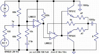
Here are Simpler Hi-Fi Audio Amplifier Circuit Diagram, If you can settle for more distortion (from about 0.2% to 0.4% at full power) and about 2.5 watts into 8 ohms with a 20 to 24 VDC power supply, the following circuit is a lot simpler. The op-amp has to discharge the base of one transistor to turn it off while also trying to pump charge into the other transistor to turn it on, hence more distortion at crossover. The distortion isn't noticeable for many applications but it's significantly higher than the circuit above. I used a larger, 2200 uF capacitor across the power. If you experience instability try adding a few hundred pF capacitor to the second op-amp from the negative input to the output. This "local" feedback should keep the op-amp happy but it might increase distortion slightly. The circuit will run on lower power supply voltage but at some point you might want to switch to a 4 ohm speaker for more volume. Applications: loud intercom, sound effects, megaphone, signal generator booster, bench amp, etc.
The NPN heat sink has mica underneath since the top layer is ground. The collector lead passes through a hole to the other side which is Vcc. The collector leads hold the transistor on one end and blobs of epoxy hold the heat sink on the other end. The holes that the various leads pass through have countersinks made by hand with a large drill to prevent shorting; you can see a blue resistor top-left in the picture is passing through to Vcc - that's the top 68k bias resistor. Also see pin 8 of the op-amp passing through to Vcc. I used a socket with long "wire-wrap" legs.
Select high gain transistors and quick op-amps that can deliver high output current to achieve the most output power. A limiting factor can be insufficient drive to the transistors for maximum output power. The transistors will be delivering over an amp at the peaks and some op-amps can't deliver as much current near the rails.
Simpler Hi-Fi Audio Amplifier Circuit Diagram
The NPN heat sink has mica underneath since the top layer is ground. The collector lead passes through a hole to the other side which is Vcc. The collector leads hold the transistor on one end and blobs of epoxy hold the heat sink on the other end. The holes that the various leads pass through have countersinks made by hand with a large drill to prevent shorting; you can see a blue resistor top-left in the picture is passing through to Vcc - that's the top 68k bias resistor. Also see pin 8 of the op-amp passing through to Vcc. I used a socket with long "wire-wrap" legs.
Select high gain transistors and quick op-amps that can deliver high output current to achieve the most output power. A limiting factor can be insufficient drive to the transistors for maximum output power. The transistors will be delivering over an amp at the peaks and some op-amps can't deliver as much current near the rails.


0 comments:
Post a Comment