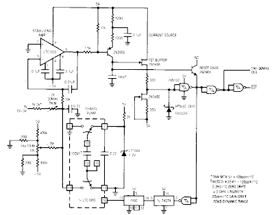
Voltage to frequency converter circuit diagram has a 1 Hz-to-30 MHz output, 150-dB dynamic range, for a 0 to 5 V input. It maintains 0.08% linearity over its entire 71/3 decade range with a full-scale drift of about 20 ppm/°C.
To get the additional bandwidth, the fast )FET buffer drives the Schottky TTL Schmitt trigger. The Schottky diode prevents the Schmitt trigger from ever seeing negative voltage at its input. The Schmitt`s input voltage hysteresis provides the limits which the oscillator runs between.


0 comments:
Post a Comment